 click to magnify
download of TNC3 and TNC31 updates
click to magnify
256 kByte EPROM will work well in TNC3. If you need more, there is a little modification necessary
TNC3S board layout (all versions including 'K) supports 128k * 8 Bit ROMs (e.g. 27C1000, AM29F010) only. Adding some wires, the 512k*8 memories may be used as well but the AM29F040 are hard to get.
1. bend pin 1 of the new EPROMs up. Socket pin 1 remains empty
2. connect both pins 1 of the EEPROM to pin 1 of one of the RAM memories.
Programming:
1. Program the new and erased flashs with TNC3-operating system (Download). Programs are made for 128 k *8 bit EPROMs but will work for 512k types as well.
2. Program the new flash-EPROMs in TNC with command flash -eo and the file OS307.abs new. Now, the flashs are ready and more files may be upladed with command flash -a .
3. UV-EPROMs should be used no more, however they CAN be used if you make a 1:1 copy of a good flash EPROM.
4. The 1 MByte flash shold be used together with the 1 MByte or 2 MByte option of TNC3 only.
Run program RS on the diskette.
Swithc TNC on and leave TF-firmware with ESC QUIT.
Prompt r:> appears.
Type first
more dip1.scr
The start script dip1.scr is displayed: e.g.
cd r:\
path r:\
rsconf 19200 1 no
tnc3boxd
Copy this file on your hard disc:
cp dip1.scr c:/dip1.scr
Change this file using any simple text editor (Notepad) according to your
requirement:
(e.g.: baud rate from 19200 to 57600) and copy the file bach into TNC31.
You can either copy the changed file into RAM (recommended):
cp c:/dip1.scr dip1.scr
or program it permanent into flash-EPROM:
flash -a c:/dip1.scr
Run program RS on the diskette.
Swithc TNC on and leave TF-firmware with ESC QUIT.
Prompt r:> appears.
Type first
more dip1.scr
The start script dip1.scr is displayed: e.g.
cd r:\
path r:\
rsconf 19200 1 no
tnc3boxd
Copy this file on your hard disc:
cp dip1.scr c:/dip1.scr
Change this file using any simple text editor (Notepad) according to your
requirement:
(e.g.: start program from tnc3boxd to rskiss) and copy the file bach into TNC31.
You can either copy the changed file into RAM (recommended):
cp c:/dip1.scr dip1.scr
or program it permanent into flash-EPROM:
flash -a c:/dip1.scr
PRELIMINARY, not tested yet
Firmware
The TNC3S / TNC31S operating system 3.08
supports the following baud rates:
75, 150, 300, 600, 1200, 2400, 4800, 9600, 19200, 38400, 57600, 115200 and
230400 baud.
Settings
The baud rates can be set using the according rsconf command or (TNC3 only) can be selected by setting the DIP-switches 1, 2 and 3:
|
DIP |
Switch 1 |
Switch 2 |
Switch 3 |
baud rate |
|
0 |
0 |
0 |
0 |
230 000 |
|
1 |
0 |
0 |
1 |
2 400 |
|
2 |
0 |
1 |
0 |
4 800 |
|
3 |
0 |
1 |
1 |
9 600 |
|
4 |
1 |
0 |
0 |
19 200 |
|
5 |
1 |
0 |
1 |
38 400 |
|
6 |
1 |
1 |
0 |
57 600 |
|
7 |
1 |
1 |
1 |
115 200 |
Hardware
Because of the MAX232A interface, the useful baudrate is limited to 115200 only. For using 230 400 baud, the MAX232A has to be replaced by MAX221. Both types are NOT pin-compatible. This makes the modification somewhat troublesome. Follow the steps below:
because in this world, you have to begin the difficult with the easy (Laotse):
remove the low pass filter C's C5 (330p) and C2 (330p) to increase RS232 bandwidth.
Now the more sophisticated operations:
Remove U7 (MAX232A) and "replace" it be a MAX221. All versions of MAX221 can be used, but you should prefer the SSOP case (suffix *AE). The *UE are TSSOP with thin metallic hairs instead of solid pins. Soldering the SSOP will be difficult enough. It may be good to add a complete RS232 level converter (including the charge pump capacitors) and to connect it with 6 wires (GND, +5, Tin, Tout, Rin, Rout) only. If J10 and J11 on the TNC3 board are opened and special pins of the 25 pin sub-d are used for the 230kbaud, the MAX232A may remain on ist place and can be re-activated again by closing only the two jumpers.
Now the list how the MAX232A pads correspond to the MAX221 pins:
| MAX232 PAD | Signal | MAX221 new |
|
1 |
C1+ |
2 |
|
2 |
V+ |
3 |
|
3 |
C1- |
4 |
|
4 |
C2+ |
5 |
|
5 |
C2- |
6 |
|
6 |
V- |
7 |
|
7 |
T2out |
n.c. |
|
8 |
R2in |
n.c |
|
9 |
R2out |
n.c. |
|
10 |
T2in |
n.c. |
|
11 |
Tin |
11 |
|
12 |
Rout |
9 |
|
13 |
Rin |
8 |
|
14 |
Tout |
13 |
|
15 |
GND |
14 |
|
16 |
Vcc |
15 |
|
15 (GND) |
\EN |
1 |
|
16 (Vcc) |
FORCEON |
12 |
|
16 (Vcc) |
\FORCEOFF |
16 |
|
n.c. |
\INVALID |
10 |
TF-parameter "W" determines the waiting time before any packet is transmitted.
The maximum delay between transmitting a packet and receiving the acknowledge
depends on the length of a typical packet, i.e. depends on baud-rate.
If slottime is set too long (Default is 100 ms), the transmitting station
will repeat the
packets before the remote station slottime-timer can send the acknowledge.
This results normally in 10 retries without waiting for acknowledge and link
failure.
Slottime should be set to 100ms with 1200 baud, 10ms with 9600 baud and 2ms
with 76k.
Using TNC3 in Hayes mode makes it possible to exchange data fully
transparent,
i.e. all 256 characters of ASCII code can be transmitted and are received
identically.
Note: The 'A' command (Auto-Linefeed) of the TF or TNC3BOX software affects
the data flow in transparent Hayes mode as well. If 'A' is set to 1 (this is
default)
with the receiving TNC, the receiving TNC adds a <LF> linefeed ($0A) after every
<CR> return ($0D). This
violates the
transparent mode and would be an unwanted
side-effect of auto-linefeed.
So, for correct transparent mode, set 'A' to 0 with both TNC before executing
the #AT
command.
The buffer length for the RS232 to TNC input buffer is 64 packets or maximum
16 kBytes. (TF version 1.87 or later)
The number of logical channels of TNC3 depends on RAM size:
| RAM size | # of channels |
| 64k (no more supported) | (20) |
| 128k (TNC31) | 50 |
| 256k (TNC3) | 50 |
| 512k (TNC31) | 100 |
| 1M (TNC3) | 200 |
| 2M (TNC3) | 200 |
Note: the table is valid for TF firmware only. With TNC3BOX and TNC3BOXD, the
number
of channels is always 10 (for the box) and 20 (for connects). With TNC3BOX, most
of the
memory space is used for Mailbox.
For outgoing data (TX), there is a maximum of 64 packets per channel
available. With 256 Bytes
per packet, this is a buffer of 16kBytes maximum. Using smaller packets will
reduce the space
accordingly. If many or all channels are in use, not all buffers can be
allocated to full length because
the RAM would limit the sum of all outgoing buffers.
For incoming data (RX), the number of buffers is only limited by total
RAM space. There is no
fixed allocation to the channels, i.e. if only one channel is used, the TNC will
buffer all data until
the RAM is full.
When using SLIP mode, the MTU is limited to 256 Bytes.
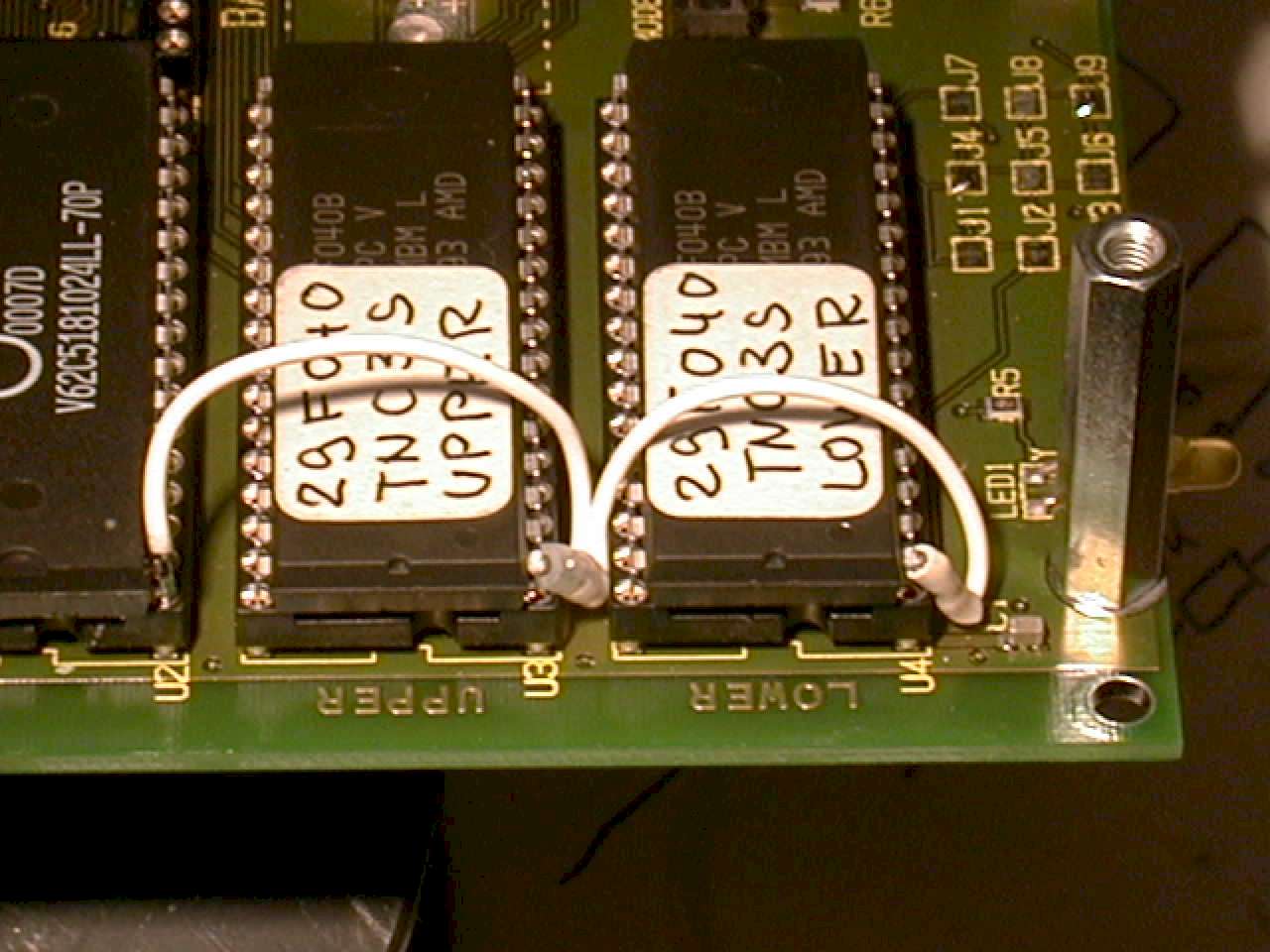
Material: 4 pcs CMOS-RAM 512kx8 Bit in DIP32 case (for 1 Mbyte 2 pcs only), 1 pcs 74C139
for skilled people. Microscope required.
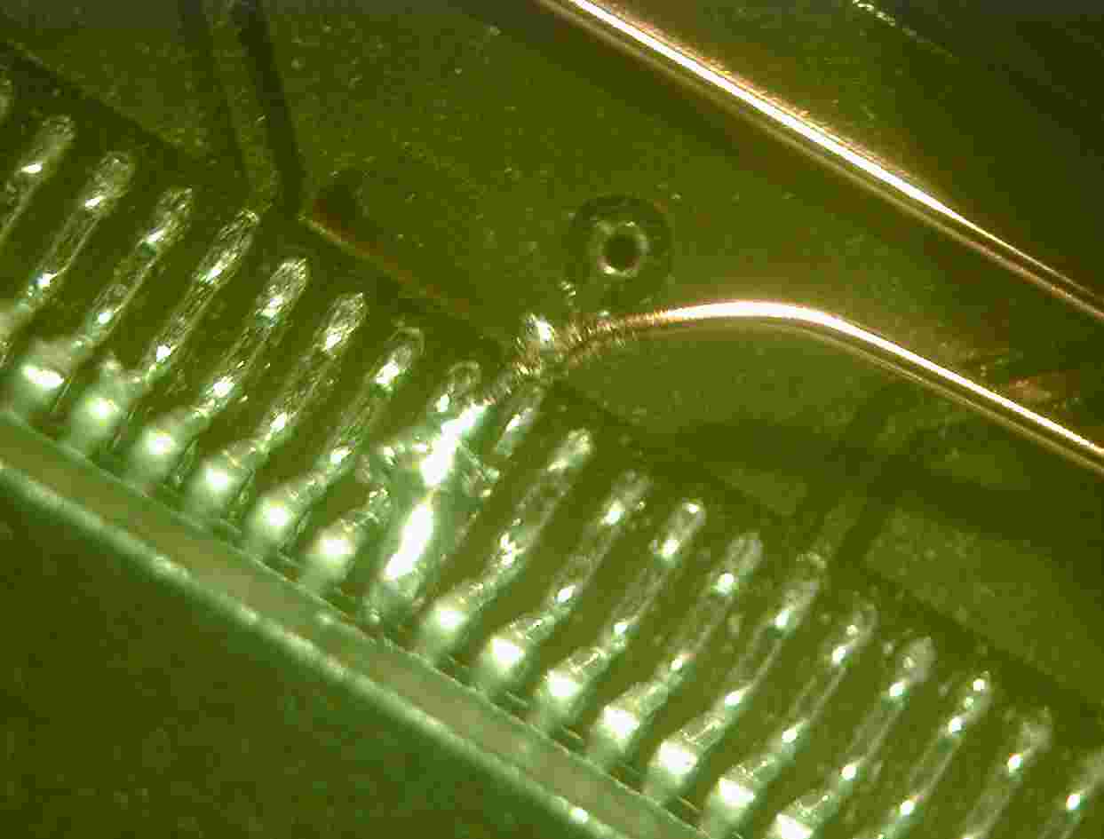
Note: Wires to Pin 22+24 of CPU are placed below the RAM-socket near pin 3, 4 and 5. Fix by a drop of glue for strain relief. Solder to CPU using a microscope.
Three RAMs (1,5 MByte) are not supported, however you may use 1, 2 or 4!
Problem: If the PC transfers large files to TNC, the transmit buffer will
overflow after 16 kByte of data.
The operating system OS309 supports hardware-handshake using RS232 RTS and CTS
wires
As these signals are NOT supported by current hardware, you have to modify it to
use the handshake.
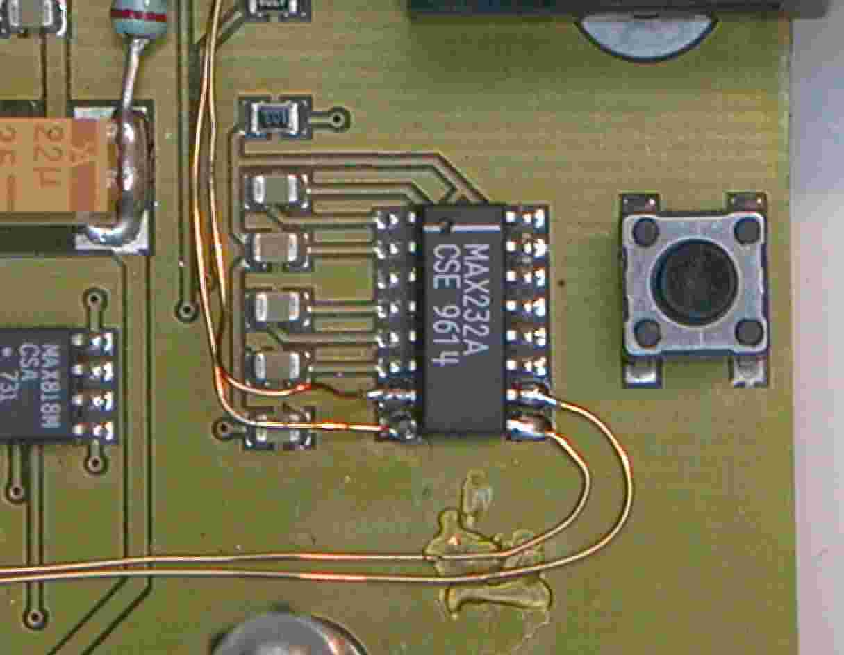
When the TNC3 cannot receive more data, (because transmit buffers are full and there is less than 256 bytes remaining), pin 66 of TNC3-CPU goes to +5 volt. Via the MAX232-driver T2 (input pin 10, output pin 7) the -10 volt RS232 signal is generated. Haveing -10 volt at pin 5 of 25-pin sub-d connector, the PC will stop transmitting data to TNC. As soon as there are 128 or less bytes in the TNC transmit buffer, pin 66 goes to 'LOW' and PC resumes transmission.
If the PC cannot receive more data from TNC (this doesn't happen normally), pin 4
of 25-pin sub-d connector goes to -10 volt. Via the RS232 MAX232 receiver R2
(input pin 8, output pin 9) the 5 volt signal to pin 49 of CPU is generated,
stopping the data flow from TNC to PC. After setting pin 49 to HI level, there
may be sent up to 10 more bytes until TNC transmission stops. As soon as pin 49
goes LOW the TNC resumes data transmission to PC.
This function exists only when the operating system command 'hwhs on' is
executed after power-on (e.g. in a .src script file DIP1.scr)
For hardware-handshake, you need the OS309 operating system and the latest TF, TNC3BOX or TNC3BOXD (Version 4.2.2001).
Hardware handshake is controlled by operating system.Default is 'hwhs off', i.e. the TNC does not care about the signals at pin 49 of CPU. If the command 'hwhs on' is executed (e.g. in script DIP1.scr), the data flow from TNC to PC can be controlled vie pin 49 of CPU. The CPU output pin 66 however will go always high as soon as the transmit buffers of TNC are full. (this does not depend on hwhs on / off)
Hardware handshake works with all programs (TF, Hayes-mode, TNC3box etc.)
1. Connect modem port 0 (middle fromt connector vorne) pin 9 (CPU pin 49 -
MCS4) to MAX232 pin 9
2. Connect modem port 0 pin 17 (CPU pin 66 - MCS3) with MAX232 pin 10
3. Connect MAX232 pin 8 with Sub-D pin 4
4. Connect MAX232 pin 7 with Sub-D pin 5
5. Connect adapter RJ45 pin 1 with SubD9 pin 1
Use a microscope!
1. Connect CPU pin 49 with MAX232 pin 9 (CPU input)
2. Unsolder (!!!) CPU pin 66 from ground pad and carefully bend up.
Connect the
IC pin to MAX232 pin 10 (have fun!) (CPU output)
3. Connect MAX232 pin 8 with RJ45 pin 7 TNC input RTS
4. Connect MAX232 pin 7 with RJ45 pin 2 TNC-output CTS
5. Connect adapter RJ45 pin 7 with SubD9 pin 7 (SubD25 pin 4)
6. Connect adapter RJ45 pin 2 with SubD9 pin 8 (SubD25 pin 5)
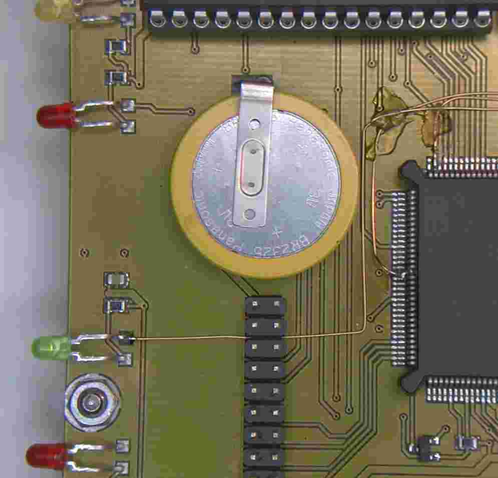
If your communications software needs a 'real' carrier-detect RS232 signal which has 'hi' level if there is a connection and a 'low' if the link is disconnected, you can abb an inverting buffer between the green CON led and pin 8 of the 25 pin sub-d connector (=pin 1 of the 9 pin type). See photos above!
As soon as a 'connect' command is executed, the green CON led lights and the minus pin of the led is pulled to zero volts. If an inverting RS232 buffer is used, you can generate an useful CD signal.
If the second transmit buffer of the MAX232 is already used for hardware-handshakeing, you have to add another RS232 driver to get the CD signal. As most computers accept a 0 Volt as 'LOW' (normally -10 volt level), you can use a simple npn-transistor or FET as inverter.
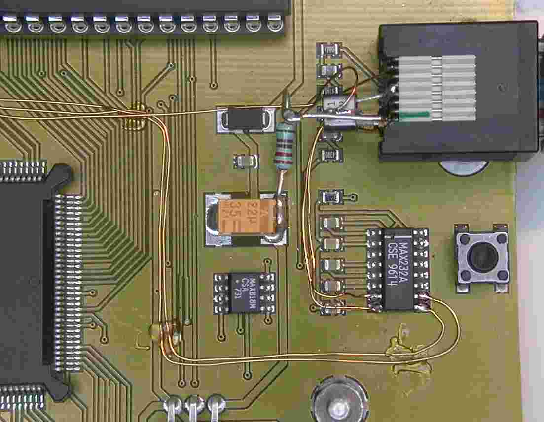
1. Connect a BS170 FET transistor: Drain to Pin 1 of RJ45 connector (marked
green on the photo)
2. Connect the source of the BS170 to ground (solder to RJ45 middle pins 4+5)
3. Connect a 2.2 kOhm resistor between C8 positive terminal (tantalum cap) and
RJ45 pin 1 (=drain)
4. Solder a wire from green DCD led cathode to the gate of the BS170.
see photos above.
For 'perfect' RS232 signals, you need a second MAX232 or a low power opamp (fed by the +/- 10 volt of the original MAX232) as driver.