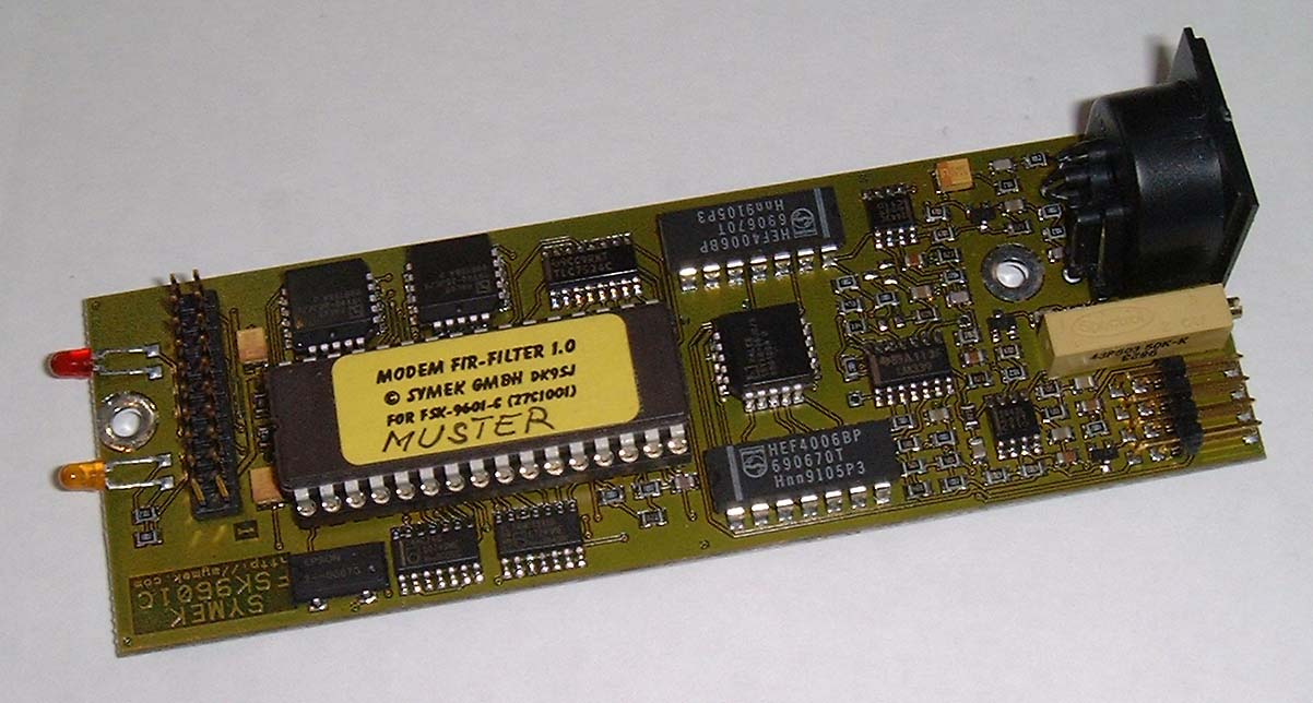
Users manual (FSK9601-C board)
Table of contents *
Preface *
Options for FSK9601 *
Technical data FSK-9601-C *
Short description *
Bit-rate and baudrate *
Digital interface - 20 pin connector *
Signal description digital interface *
Connecting the FSK9601 to general TNC2 *
Connecting the radio to FSK9601 *
Modulator (Pin 1) *
Demodulator (Pin 4) *
PTT (Pin 3) *
GND (Pin 2) *
Standard FSK connection cable *
TRX4S, Kenwood, Yaesu, Azden etc. *
TEKK KS960 Tnet Mini *
Settings and adjustments of modem FSK9601 *
Jumpers FSK9601 *
Bit-Error-Test (Jumper 1) *
Permanent transmit on PTT (jumper 2) *
FSK / GMSK switch (jumper 3) *
Filter-select switch (jumper 4) *
Solder programmable jumpers in modem FSK9601 *
Watchdog (solder jumper 16) *
Jumper J17 "RX-muting" *
Jumpers for selecting the baudrate" *
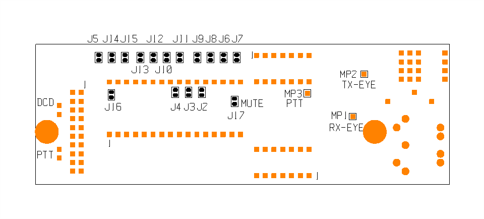
Test pins on modem FSK9601 *
Setting the Baudrate with FSK9601 *
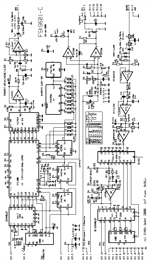
Schematics Modem FSK9601-C *
Component Location Modem FSK9601-C *
Copyright for Hard and Software *
This manual should help you to use the FSK-Packet-Radio-Modem FSK9601 in your TNC3 or TNC31 controller and to install the connection to your radio transceiver. If there are any problems, you may ask for help
via e-MailWith this manual, the expression "FSK9601" is used. However, all parts of the manual are valid for the various options of FSK9601 for baudrates from 4800 up to 614 kBaud as well.
If you need instructions how to modify a specific amateur radio transceiver for 9600 baud operation, ask us. We have a collection of many plans how to modify the transceivers. Write us an e-mail, we shall reply and attach the information requested if possible.
The FSK9601 board is tested and ready for use in the TNC3 or TNC31. For use with other packet-radio-controllers, it may be necessary to use an additional 20 wire ribbon cable. The data exchange between TNC3/31 and the modem is NRZI-formatted. If you want to use the FSK9601 with a TNC2, you need to order the option 'NRZ' because here the data format is NRZ. The difference between standard NRZI and optional NRZ version is only the programming of two of the three GALs. They are marked 'R', 'T' and 'C' for the optional NRZ version. The GALs cannot be changed, so you have to order the modem with 'Option NRZ-GAL'
Most power of FSK9601 is consumed by the GALs. There are versions with 'zero-power-GALs' available, which reduce the total supply current of the modem from 115 to 30 mA at 5 volt. The GALs cannot be changed, so you have to order the modem with 'Option Zero power GAL'
Standard speed options for FSK9601 range from 9600 to 307200 Baud. Receive and transmit baudrate may be different with one modem, e.g. the combination receive 38400 and transmit 9600 is common for satellites with fast downlink data rates.
Receive baudrates from 2400 to 1228800 Baud and transmit baudrates from 9600 to 614400 Baud are possible.
Odd baudrates (not a 2n multiple of 2400 Baud) are available on special request.
Power supply:
5 volt DC, typ 125 mA. (Option low-power: 30 mA) typical values.
Dimensions:
ca. Length=120mm, Width=41mm, Height=25 mm, mass approx. 45 grams
Radio interface:
5-pin DIN connector, same pinning as TNC2, TNC2S, TNC2H etc. Modulation (filter, scrambler) according to specifications of G3RUH, speed: 9600 baud / 9600 bit/s (optional other baudrates).
AF-output level adjustable from 10 mVpp to 3.5 Vpp, Ri: 2kW , DC-free. (up to 6 V DC permissible). Output is muted while reception. PTT : max. 25V 0,1A to ground, input sensitivity: 100-700 mVpp at 100 kW , DC-free. A input limiter (0,5Vpp) avoids overdriving the amplifiers by short DC peaks at T/R switching.
NF-filter:
8 bit wide, 512-tap FIR-Filter in the transmitter with 64-fold oversampling (DK9SJ-type). Active lowpass filters in TX and RX. All inputs and outputs to the radio are filtered with R-C-R filters for EMI suppression. A FSK-filter (raised cosine rolloff) and a GMSK filter are selectable by a jumper.
Modem interface (digital):
CMOS -level 5 volt. TXData, TXClock, RXData, RXClock, RTS CTS, DCD, + 5 volt,
reset, ground. Connector: 20 pin (2x10) ribbon connector.
LED display:
DCD (carrier detect), PTT (transmitter keying)
Jumpers and trimmers:
4 jumpers for PTT-keying, bit-Error-test, FSK/GMSK filter and spare filter select. Setting of output voltage with a 20 turn trimmer.
Watchdog:
The PTT-switch is time-limited to approx. 15 seconds. In case of failure of the TNC, the PTT is released after the maximum time. For tests or special applications (digipeaters with long transmission periods) the watchdog may be disabled by a solder jumper.
Jumpers on board:
AF-output muting on/off, baudrate 9600 / 19200 / 38400 / 76k8, 153k, 307k Baud, watchdog disable. Different TX and RX baudrates are selectable.
A 'modem' contains modulator and demodulator circuits.
The FSK9601 converts the digital signals of a packet-radio-controller to low-frequent tones, which can be transmitted by a FM radio. Further, it decodes the tones received by a FM radio and sends them to the packet radio controller in digital form.
The modem FSK9601 generates and receives AF signals according the G3RUH-recommendations, which is usual with amateur radio on terrestrial and satellite links. all frequencies are quartz controlled, adjustments are not necessary. The audio bandwidth of the signal goes from 30 Hz to 5000 Hz (9600 bit/s. With other baudrates, the bandwidth is higher or lower according to the speed.)
The transmit clock frequency (9600 Hz) is generated in the modem. The modem includes also the circuitry for transmitter-keying (PTT) and transmit-time limiter (watchdog).
In this manual, the expressions bit-rate (bit/s, bit per second) and baud (Bd) are used for determining the transmission speed. With the FSK9601 both values are equivalent, as there is exactly 1 bit transmitted with every clock cycle. In general, it is possible to transmit more than 1 bit per clock, the speed (in bit/s) is then a multiple of the clock rate.
Digital interface - 20 pin connector
|
Pin |
Signal |
Function |
Pin |
Signal |
|
1 |
+ 5 Volt |
power supply 5 volt 150 mA (from TNC) |
2 |
Ground |
|
3 |
+ 5 Volt |
power supply 5 volt 150 mA (from TNC) |
4 |
Ground |
|
5 |
Reset |
(not used in FSK9600) |
6 |
Ground |
|
7 |
DCD |
AF carrier detect (from modem to TNC) |
8 |
Ground |
|
9 |
CTS |
transmitter is keyed (from modem to TNC) |
10 |
Ground |
|
11 |
PTT |
transmitter keying (from TNC to modem) |
12 |
Ground |
|
13 |
TXD |
transmit data (from TNC to modem) |
14 |
Ground |
|
15 |
RXD* |
receive data (from modem to TNC) |
16 |
Ground |
|
17 |
TXC |
transmit clock (from modem to TNC) |
18 |
Ground |
|
19 |
RXC* |
receive clock (from modem to TNC) |
20 |
Ground |
*: RXD and TXD can be encoded NRZ as well as NRZI.
Signal description digital interface
Reset (Pin 5): (modem input) normally high, is pulled low for 50 ms at power-on of TNC3. (not used in FSK9601)
DCD (Pin 7) Data Carrier Detect: (modem output) High: modem receives no carrier, low: modem has locked on a G3RUH-signal.
CTS (Pin 9) Clear to Send: (modem output) Normally high. If the modem is ready to transmit data, the signal is low. With the FSK9600, CTS output is connected to PTT input. The TNC will wait for CTS=low before data transmission starts.
PTT (Pin 11) Push to talk, or RTS (Request to send): (modem input) normally high. When the transmitter is to be keyed, the TNC pulls this signal to low.
TXD (Pin 13) Transmit Data: (modem input): The data is latched at rising edge (low to high transition) of transmit clock.
RXD (Pin 15) Receive Data: (modem output): The data output changes at the falling edge and is valid at the rising edge (low to high transition) of the receive clock.
TXC (Pin 17) Transmit Clock: (modem output): The modem generates a clock frequency, which determines the transmit baudrate and the data speed between TNC and modem. Transmit data signal TXD has to be stable at the rising edge of TXC.
RXC (Pin 19) Receive Clock: (modem output): the output of the receive clock recovery circuit is sent to the TNC to synchronise the received data signal. RXD is stable at the rising edge of RXC. The frequency of RXC corresponds to the transmit clock of the remote transmitter. If the internal clock of the modem and the clock of the remote transmitter differ by some percent, the receive clock is adjusted by 1/32 clock cycle to maintain synchronism.
Connecting the FSK9601 to general TNC2
If the FSK9601 is to be used with a TNC2, the 6 signals are connected to the Z80-SIO as follows: (Pinning refers to 40 pin Z80-SIO)
SIO-Pin 9 ----------- Modem Pin 1 and 3 (+ 5 Volt)
SIO-Pin 19 ----------- Modem Pin 7 (DCD)
SIO-Pin 18 ----------- Modem Pin 9 (CTS)
SIO-Pin 17 ----------- Modem Pin 11 (RTS)
SIO-Pin 13 ----------- Modem Pin 13 (TXD)
SIO-Pin 12 ----------- Modem Pin 15(RXD)
SIO-Pin 14 ----------- Modem Pin 17 (TXC)
SIO-Pin 13 ----------- Modem Pin 19 (RXC)
SIO-Pin 31 ----------- Modem Pins 2,4,6...20 (GND)
Note: for 9600 baud operation, the system clock of the TNC2 should be 10 MHz or higher. The NRZ-option GALs of the FSK9601 must be used.
As the G3RUH-modem includes a scrambler, it would make no difference in transmit spectrum if NRZ or NRZI is used. However, to keep all systems compatible, the NRZ and NRZI versions have to be observed. Using two modems with the 'wrong' GALs would result in the same perfect communication, however other modems with the 'correct' NRZ/NRZI setting cannot read this signals.
Connecting the radio to FSK9601
Connecting a 9600 baud FSK modem to a radio requires modification of the radio in most cases. You have to find a suited point in the transmitter circuit to modulate the transmitter without significant distortion. The receiver circuit has to be tapped directly after the demodulator to get an unfiltered signal.
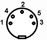
For connecting the radio, use a 5 pin DIN connector (180 degree pinning). The five pins are numbered as shown: (view to solder side of plug, view to front of the socket):
Pin 1: MODULATOR of radio, output of modem
Pin 2: GND ground
Pin 3: PTT transmitter keying, push-to-talk contact to ground
Pin 4: DEMODULATOR output of radio, input of modem
Pin 5: N.C.
Note: the five pins are not enumerated in turn.
Here, the modulator of the radio is connected. The maximum output voltage of the modem is up to approx. 3.5 Voltpp and could be adjusted with the only trimmer resistor (accessible at the rear side of TNC3/31). The minimal output voltage, which could be set, is about 10 to 20 mV. Below this, the adjustment becomes somewhat fiddly. The modem has a output amplifier with a series output resistance of 2 kW .
Sometimes, the radio requires much less AF-voltage, e.g. only 10 mV for sufficient modulation. For this case, the AF voltage must be reduced by a voltage divider, which should be placed in the radio. The output of the modem should be about 1 Volt for good adjustment with the pot near middle position. This gives less susceptibility to hum and noise. Another fine place for the voltage divider is the DIN-plug.
The output voltage is coupled via an electrolytic capacitor. There should be no DC voltage applied to pin 1, which is more positive then 2.5 Volt because the output capacitor of TNC will be reversed in polarity. If the modulation input of your radio shows more voltage, you should connect a 10µF capacitor in series, minus connection directed to the modem. The transmit signal sounds like white noise, but on a oscilloscope you recognise pulses with a distance of about 0,1 ms. (at 9600 Baud)
IMPORTANT: the correct adjustment of the transmit AF is very important. As the radios are modulated directly (there is no AF-amplifier or modulation limiter), you may far overdrive the modulator by applying too much AF voltage. This gives the transmit signal an excessive bandwidth and the IF filter of the destination receiver will totally distort the signal. We advice to watch closely the eye diagram at the receiver and adjust then the proper modulation level. If the AF is too low, you may loose some signal-to-noise ratio, but you don't risk to distort the signal by overdriving.
The demodulator-output of the radio is connected to this pin. The AF voltage should be 150 mV or more. The decoder works at voltages of 50 mV or more without errors, but the DCD-LED will flicker and the modem is sensitive against signal distortions.
If the output of your radio produces much more signal voltage, it should be reduced by a voltage divider, which is mounted in the radio to get 0.7 Volt or less. The input resistance of the modem is about 100 kW in parallel with the input filter capacitance (100 pF).
Input voltages exceeding 1 volt are limited by a diode pair, causing excessive distortion of the signal. Make sure not to overdrive the input to avoid this.
This pin is switched to ground when transmitting. With this, all common PTT-circuits of the usual radios may be operated. The switch in the TNC is a n-channel vertical MOS-field effect transistor (VMOS-FET), which is able to switch up to 25 Volts and up to 250 mA. In the 'on'-state, the resistance of the FET is typically 30 W or less, the cut-off current when switched off is far below 1 µA. VMOS-FETs are suited well for such applications, because the voltage across the switched-on FET is low (only a few mV). Bipolar silicon npn-transistors have usually saturation voltages, which are much higher.
With this circuit, it is only possible to switch DC-voltages up to about 20 Volts to ground. You cannot pull a line up to 12 Volt when transmitting or switch a negative voltage. For this application, you should use a switching amplifier or a reed relay (with diode clamp).
At most (handy) radios, the PTT contact and microphone is connected to the same signal pin. The AF-path for the microphone signal is decoupled by a series capacitor, the PTT-signal is fed by a series resistor of 2 to 20 kW in order not to short-circuit the microphone. When pressing the PTT switch, DC current may flow through this resistor, keying the transmitter. As the microphone will not be used with the 9600 Baud FSK-modem, the mic-connector of the radio may be connected directly to the PTT-pin of the modem. Then, the short circuit of the mic-modulation is no disadvantage.
Ground of the radio (case, 0 Volt)
for transceivers with 9600 Baud FSK Capability
Since about 1994, the industry begun to produce amateur radio transceivers with the necessary inputs and outputs for 9600 Baud FSK. The transceivers of Kenwood, Azden Alinco, Yaesu, ICOM, SYMEK use the same connector and pinning and are easy to connect to a FSK9600. The radios have a 6 pin mini-DIN socket (same type as for PS/2 keyboards). You have to make a simple cable with a 6 pin jack on the one side and the 5 pin DIN jack on the other. Just connect the pins 1 to 1, 2 to 2, 3 to 3 and 4 to 4. Pins 5 (and 6) remain unconnected. As it is difficult to solder the tiny 6 pin jack it is better to buy a ready-made PS/2 keyboard extension cable, cut it into two pieces and attach the 5 pin DIN connector to the open end. Read the manual of the radio, how the FSK mode is to be enabled and how to adjust sensitivity. If the demodulator output voltage exceeds 0.5 volt, it is a good idea to reduce it to that level by soldering a voltage divider into the cable plug.
TRX4S, Kenwood, Yaesu, Azden etc.
TRX4S, TM733, TM455, TM251, TM451, TM-V7E, Azden PCS9600, Yaesu FT8500 etc. with 6 pin mini-DIN DATA-socket:
Modem Pin 1 (MOD) radio Pin 1 Data in, packet data input
Modem Pin 2 (GND) radio Pin 2 Ground
Modem Pin 3 (PTT) radio Pin 3 PTT, 'standby'
Modem Pin 4 (DEMOD) radio Pin 4 Data out, 9600 Baud packet output
9-pin sub-D plug (socket at the transceiver)
Modem Pin 1 (MOD) radio Pin 4 Transmit Data in
Modem Pin 2 (GND) radio Pin 2 Ground
Modem Pin 3 (PTT) radio Pin 3 PTT Line
Modem Pin 4 (DEMOD) radio Pin 5 Receive Data out
Reduce data out voltage via a 1:3 voltage divider (22 kW in series, 10 kW parallel) to 0,5 volt.
Settings and adjustments of modem FSK9601
Note: the modem board is built-in in the TNC3 or TNC31 bottom-up (component side down). The following description shows the modem board with the component side down! Jumper 1 is near the edge of the modem board, the jumper 4 is located with 4 to 5 mm distance to the modulation amplitude trimmer.
The jumpers are closed by normal 2,5 mm jumper bridges. Unused jumpers may be plugged parallel to the board edge on the pins which are nearest to the board. All these pins are connected to ground.
¢ = jumper installed
: = no jumperNormal mode: The modem is shipped with no jumpers active. The jumpers are plugged parallel to the board on the ground pins.
|
(DIN-Connector) (Trimmer) |
4 |
3 |
2 |
1 |
|||||
|
· |
· |
· |
· |
||||||
|
· |
· |
· |
· |
Normal mode: FSK
To run the bit-error-test ("BERT"), the transmitter is set to 'permanent zero' transmission. Check at the remote receiver, for 'ones': Every pair of 'ones' represents a transmission error. BERT is useful for test and adjustment of the signal path.
NOTE: if jumper 1 os closed, no ndata can be transmitted. However, the TNC may key up the transmitter and apparently data is sent. But with BERT jumper installed, this data contains no information and no connect is possible.
|
(DIN-Connector) (Trimmer) |
4 |
3 |
2 |
1 |
|||||
|
· |
· |
· |
· |
||||||
|
· |
· |
· |
· |
Bit-Error-Test mode enabled
Permanent transmit on PTT (jumper 2)
With jumper 2, the PTT of the radio may be keyed. This is used for tests and adjustment. The transmit time limiter (Watchdog) is not in effect when keying the PTT by jumper 2. For normal operation, set jumper 2 always 'OFF'!
For testing, it makes sense to install jumper 1 (BERT) and jumper 2 (transmit) at the same time.
As long as the transmitter is keyed (by TNC command or by jumper 2), the modem-transmitter is NOT muted.
|
(DIN-Connector) (Trimmer) |
4 |
3 |
2 |
1 |
|||||
|
· |
· |
· |
· |
||||||
|
· |
· |
· |
· |
permanent transmit ON
With jumper 3, the transmit characteristic can be switched from the usual FSK-modulation to GMSK. Both modulation types are alike, if there is not much noise present, you will find no difference. For best results, use the FSK-filter (jumper not installed).
|
(DIN-Connector) (Trimmer) |
4 |
3 |
2 |
1 |
|||||
|
· |
· |
· |
· |
||||||
|
· |
· |
· |
· |
GMSK-Filter enabled
Filter-select switch (jumper 4)
The filter-EPROM can store up to four different sets of filter coefficients. Standard is FSK and GMSK-operation. Two additional filter curves may be selected by installing jumper 4. With the standard modem, this has no effect (future use)
|
(DIN-Connector) (Trimmer) |
4 |
3 |
2 |
1 |
|||||
|
· |
· |
· |
· |
||||||
|
· |
· |
· |
· |
Optional filter enabled (future use)
Solder programmable jumpers in modem FSK9601
For special applications, there are some solder jumpers on the bottom side of the FSK9601 board. To open soldered jumpers, carefully remove the solder with desolderung wick. J6 and J17 are closed by a copper trace, which has to be cut' with a small sharp knife.
Bottom side (solder side) of the printed circuit board FSK9601-C
The FSK9601 modem will key a transmitter only for a limited time. If the watchdog timer (approx. 15 seconds) is expired, the PTT is released and the transceiver returns to receive mode, even when the TNC keeps the PTT-control line to 'low'. So, it can be made sure, that the TNC does not key up the transmitter permanently, even in case of a software malfunction. This circuit is called Watchdog.
For full duplex or digipeater use, this watchdog function may be disabled by soldering jumper J16. This may be also useful for some tests, if the transmitter is to be keyed up for longer periods. With jumper 2 (see above), the transmitter may be keyed up independantly from the watchdog setting.
In receive mode, the transmitter (modulation output) of the modem is muted. (Jumper MUTE installed). If a signal has to be generated even in receive mode, the trace J17 has to be removed.
Jumpers for selecting the baudrate"
For setting the transmit or receive baudrate, you have to change not only the jumpers but some components of the analog filters too. However, we explain the function of the related solder jumpers here:
|
TXBaud |
9600 |
19200 |
38400 |
76800 |
153600 |
307200* |
307200+ |
614400+ |
|
|
|
|
|
|||||||
|
RX 2400 |
J2 + J6 |
||||||||
|
RX 4800 |
J3 + J6 |
J2 + J8 |
|||||||
|
RX 9600 |
J4 + J6 |
J3 + J8 |
J2 + J10 |
||||||
|
RX 19200 |
J5 + J6 |
J4 + J8 |
J3 + J10 |
J2 + J12 |
|||||
|
RX 38400 |
J9 + J6 |
J5 + J8 |
J4 + J10 |
J3 + J14 |
J2 + J14 |
J2+J12 |
|||
|
RX 76800 |
J11 + J6 |
J11 + J8 |
J5 + J10 |
J4 + J12 |
J3 + J14 |
J2 + J14 |
J3+J14 |
J2+J14 |
|
|
RX 153k |
J13 + J6 |
J13 + J8 |
J13 + J10 |
J5 + J12 |
J4 + J14 |
J3 + J14 |
J4+J12 |
J3+J14 |
|
|
RX 307k |
J15 + J6 |
J15 + J8 |
J15 + J10 |
J15 + J12 |
J5 + J14 |
J4 + J14 |
J5+J12 |
J4+J14 |
|
|
RX 614k* |
J15 + J6 |
J15 + J8 |
J15 + J10 |
J15 + J10 |
J5+J14 |
||||
|
RX 614k+ |
J13 + J6 |
J13 + J8 |
J13 + J10 |
J5 + J12 |
J3 + J14 |
J4+J12 |
|||
|
RX 1228k+ |
J15 + J6 |
J15 + J8 |
J15 + J10 |
J5+J14 |
J15+J12 |
*: Xtal oscillator 19,6608 MHz instead of 9,8304 MHz
+: Xtal oscillator 39,3216 MHz instead of 9,8304 MHz
You can access three test pins on the bottom side of the modem board:
MP1 (RX-Eye): AF-signal at the decider (comparator) input. Connect an oscilloscope to check the receiver eye diagram. s an.
MP2 (TX-Eye): Transmit signal at the D/A converter output. , unfiltered, transmit-eye diagram. Check the transmit-eye before the antialiasing filter and modulation amplitude trimmer.
MP3 (PTT): MP3 is LOW (0 Volt) in receive mode, HIGH (+ 5Volt) in transmit mode.
Setting the Baudrate with FSK9601
The FSK9601 is available for various baudrates from 1000 Baud to 1,228 kBaud, baudrates of transmitter and receiver can be configured to be different.
For setting the baudrate, it is necessary to:
| select the frequency of the master clock oscillator | |
| set the frequency dividers with the solder jumpers J2 to J15 | |
| select the component values of the analog transmit and receive filters according to the baudrates. |
Changeing the baudrate requires tools for smd part soldering and experience in handling such miniature parts. We do not recommend to change the baudrate. We shall publish the instructions for changeing baudrate on
http://symek.com later.Known problems
A white noise spectrum contains components, which are recognised by the DCD circuit of the FSK9601 as valid data signal. This cannot be avoided and may cause the DCD led to flash sometimes even if there is no data signal present.
If there is absolutely NO signal at the input (short circuit, no noise), it may happen that the last state of the DCD remains 'ON' until there is a new signal at the input. The input signal should therefore be unsquelched, otherwise the transmitter could be blocked due to an apparent busy channel. Countermeasures: A 1 MOhm resistor could be soldered parallel to R35.
Component Location Modem FSK9601-C
E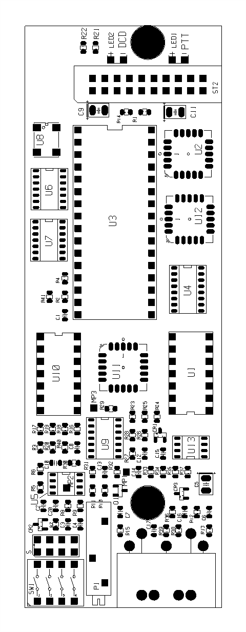
Copyright for Hard and Software
There exists a copyright for the FIR filter EPROM to SYMEK GmbH or Ulf Kumm, DK9SJ.All other copyrights for schematics and board-layout belong to SYMEK GmbH or Ulf Kumm, Stuttgart. The modem cannot be operated independently. So, it is a complex component and there is no need for a EMI certification (CE-sign). When the modem is to be used in systems other than TNC3 or TNC31, the EMI regulations have to be observed. The contents of this manual may be copied as long as the author and the source is mentioned.